

Substantial Chip Resistor Selection Guide for High-Power Circuit Applications
2026-07-09
Selecting the right chip resistor for high-power circuits is far from trivial—thermal management, pulse handling, and long-term stability demand careful consideration. Milliohm brings clarity to this challenge with a guide that cuts through the noise, offering practical insights you won’t find in generic datasheets. Whether you’re pushing current limits or optimizing board space, the choices ahead will define your design’s reliability.
Translating Thermal Demands into Resistor Form Factors
Every circuit has a thermal story, and resistors are central characters in that narrative. The challenge isn’t just selecting a resistor that can handle a given wattage on paper—it’s about anticipating how heat will flow, accumulate, and dissipate within the actual physical layout. A resistor’s form factor, from the material of its core to the geometry of its leads, directly shapes this thermal behavior. For instance, a wirewound resistor in a ceramic boat package may excel at conducting heat away to a heatsink, while a thick film chip resistor relies on surface area and PCB copper pours for cooling. Recognizing these differences early prevents overdesign and hotspots that degrade reliability.
Board-level constraints often flip the script on resistor selection. Picture a dense power supply where components sit shoulder to shoulder: the resistor’s physical size isn’t just about power rating—it dictates airflow paths and influences the temperature of nearby capacitors. A taller, narrower metal-oxide film resistor might shed heat through convection better in a cramped space, while a flat, wide SMD shunt resistor could spread its thermal load across a ground plane. Designers need to think beyond datasheet numbers and visualize how a component’s silhouette interacts with the rest of the board. Sometimes a seemingly oversized resistor is the only way to keep an adjacent sensitive IC within its safe zone.
Manufacturing technologies also leave distinct fingerprints on a resistor’s thermal footprint. Laser-trimmed thin film parts, for example, can develop micro-hotspots along their resistive path if the trimming creates narrow current channels. In contrast, bulk metal foil resistors with a flat, homogeneous element distribute stress and heat more uniformly, allowing tighter long-term stability without the same localized temperature spikes. Even the lead frame or termination style matters—a resistor’s ability to flex during thermal cycling can reduce solder joint fatigue. By matching the physical form to the expected thermal demands, engineers can build in resilience that pays off over years of field operation.
Material Choices That Dictate Power Dissipation
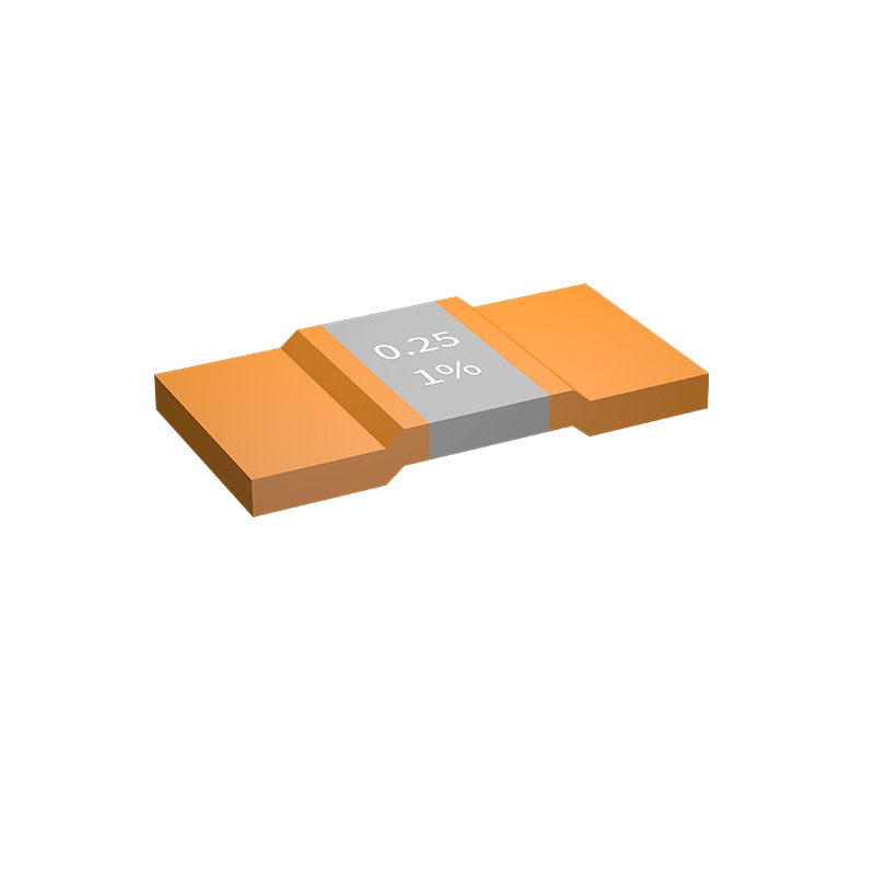
The power dissipation of any electronic component hinges on the materials from which it is built. Take the substrate as a starting point: traditional silicon wafers have been the backbone for decades, but their inherent resistivity and thermal limitations become glaring as we push for higher frequencies and smaller form factors. Wide-bandgap alternatives like silicon carbide and gallium nitride sidestep many of these pitfalls. Their higher critical electric fields allow for thinner device layers that slash conduction losses, while superior thermal conductivity whisks heat away more effectively, keeping junction temperatures in check even under heavy loads. The choice here isn't just about efficiency—it's about preventing thermal runaway and ensuring long-term reliability.
Beyond the semiconductor itself, the metals used for interconnects and contacts play an equally critical role. Aluminum has been a workhorse, but copper’s lower resistivity directly reduces I²R losses in power delivery paths. As current densities climb, even minor differences in material conductivity translate into significant gains. Yet copper alone isn't a silver bullet; it requires careful barrier layer engineering to prevent electromigration, which can degrade performance over time. Innovations like cobalt capping and ruthenium liners are quietly extending the practical limits of current-carrying wires, directly impacting how hot a chip runs under sustained operation.
Then there's the often-overlooked realm of packaging and thermal interface materials. Solder compositions, die-attach adhesives, and even the ceramic substrates that bear the entire assembly all have their own thermal resistances. A shift from standard silver-filled epoxies to sintered silver can dramatically lower the thermal impedance between the die and its heat spreader. Similarly, moving from alumina to aluminum nitride for the package base can double the thermal conductivity, easing the path for heat to escape. These seemingly minor substitutions collectively shape the thermal budget, dictating whether a design can hit its performance targets without throttling or failure.
Footprint Economics: Balancing Board Space and Heat Spreading
Every square millimeter of a printed circuit board carries a cost that goes beyond the bill of materials. When power components demand generous copper pours for thermal relief, the real expense isn't the copper itself—it's the territory conquered. A design that sprawls across the board to keep temperatures in check may inadvertently force larger form factors, pricier enclosures, and more complicated assembly, all of which eat into margins in ways that a simple component price list never reveals.
The tension between footprint and thermal performance often hides in plain sight. Designers who default to oversized pads and expansive ground planes for every hot part may feel prudent, but they're paying a premium for peace of mind. Smart footprint economics starts with questioning those defaults. Could a smaller outline home for that regulator still meet the thermal budget if paired with vias-in-pad and a carefully considered stackup? Often, the answer is yes—but it requires moving past rule-of-thumb layouts and into simulation-driven trade-offs that treat board space as a currency worth spending intentionally, not lavishly.
Getting this balance right isn't simply about cramming components closer together. It demands a mindset that views thermal dissipation and spatial constraints as intertwined variables rather than opposing forces. By optimizing not just where heat sinks connect, but how heat paths are sculpted through the board’s layers, engineers can shrink footprints without sacrificing reliability. The payoff is a design that runs cooler in a tighter envelope, proving that when footprint economics is done well, thermal management becomes a feature of the layout rather than a costly afterthought.
Current-Sense Precision Under Thermal Stress
Thermal stress can quietly erode the precision of current-sense circuits, even when everything looks fine on paper. A resistor might boast a tight tolerance at room temperature, but once it heats up, its temperature coefficient of resistance (TCR) can introduce drift that no amount of calibration at 25°C can fix. This isn’t just about the sensing element itself—the PCB traces, solder joints, and nearby power components all play a role in creating localized hotspots that throw off the measurement.
When you push a design to its thermal limits, the interplay between self-heating and ambient temperature changes becomes critical. A current-sense amplifier’s input offset drift, for instance, often follows a nonlinear curve that datasheets struggle to capture in a single number. Pair that with a shunt resistor whose TCR varies across its operating range, and the combined error can easily exceed 1% or more, especially in high-current paths where even a few milliohms of extra trace resistance matters.
Designers who rely solely on simulation or bench testing at a constant temperature often miss these effects until prototypes fail in the field. Subtle layout choices—like placing a sense resistor too close to a voltage regulator or running a high-current plane underneath—can create thermal gradients that shift over time. The fix usually involves a mix of derating, distributed sensing points, and sometimes active compensation, but the hard part is catching the issue before it turns into a field return.
Pulse-Handling and Surge Robustness in Dense Layouts
When components are packed tightly together, the interplay between surge events and physical proximity takes center stage. Parasitic coupling that barely registers in spacious designs can suddenly dominate in high-density layouts, creating unintended conduction paths during fast transients. The challenge isn't just about selecting parts with high pulse ratings—it's about predicting how those pulses will flow through the inevitable stray capacitances and mutual inductances that emerge when guard rings overlap and spacing rules get pushed to their limits.
Thermal stacking further complicates the picture, because dense boards trap heat that magnifies resistance shifts and accelerates failure mechanisms. A surge that a device might comfortably shrug off on an open test bench can push the same component past its safe operating area when surrounded by other heat-dissipating elements. Effective pulse robustness here depends on a systematic analysis of the entire current loop, from the input clamping network right down to the ground return paths, making sure no narrow trace becomes a fuse under a fast-rising edge.
Clever placement of polyfuses and transient voltage suppressors helps, but true resilience comes from treating the layout itself as part of the protection circuit. Adding small amounts of intentional impedance—whether through carefully sized ferrite beads or controlled trace inductance—can steer destructive energy away from sensitive nodes without bloating the footprint. Iterative co-simulation of electromagnetic and thermal models has become essential, letting engineers spot the hotspots where a layout’s density amplifies surge stress before the first prototype ever hits the bench.
Designing for Reliability: Derating Beyond the Datasheet
When engineers first learn about derating, it often sounds deceptively simple: pick a component rated for twice the expected stress and move on. But in practice, meaningful derating demands a much deeper understanding of failure mechanisms that datasheets only hint at. A capacitor’s voltage rating might look generous on paper, yet under continuous bias at elevated temperatures, its dielectric can degrade faster than accelerated life tests suggest. The key is to model not just the average stress, but the tails of the distribution—transients, ripple currents, and thermal cycling that accumulate subtle damage long before any parametric shift appears in a datasheet plot.
Going beyond the datasheet means engaging with application-specific physics. For instance, a resistor’s power derating curve assumes a certain ambient temperature and free-air convection, but if that part sits next to a hot-swap controller or is conformally coated inside a sealed enclosure, the local thermal resistance can double. Similarly, derating a MOSFET by current alone overlooks the silent killer of repeated avalanche events during inductive switching—a stress often absent from standard SOA curves. Robust designs treat derating factors as living parameters, refined through prototyping, infrared imaging, and accelerated margin tests that probe the real boundaries of failure.
The most reliable systems emerge when derating becomes an architecture-level concern rather than a component-level checkbox. That means allocating margin not just in static ratings but in timing, signal integrity, and software guard bands. It requires reading between the lines of qualification reports, asking whether the datasheet limits reflect true wear-out or merely test capability, and recognizing that cumulative stress—like repeated inrush surges into a bulk capacitor—rarely follows the single-event surge rating. By treating datasheet numbers as starting points rather than guarantees, design teams uncover vulnerabilities that standard derating tables never capture, ultimately building products that outlast their paper specifications.
FAQ
Power rating and thermal resistance are the starting point. You need a resistor that can dissipate the expected heat without exceeding its maximum operating temperature. Look closely at the pulse handling capability if your circuit experiences surges or inrush currents. The voltage coefficient of resistance matters when operating near the maximum voltage limit, as some materials drift under high field stress. Also, don't overlook the resistor's construction — thick film, thin film, and metal foil each behave differently under sustained high loads. Finally, check the temperature coefficient of resistance (TCR) to ensure stability across your operating range.
Pulse performance is critical because many high-power circuits don't draw steady current. A resistor might handle 5 W continuously but fail instantly with a short 50 W spike. The key metric is energy absorption per pulse, often given in joules for a specific pulse shape. It depends on the resistive element's thermal mass and the uniformity of the current path. Look for resistors rated with pulse-specific data, and calculate your worst-case pulse energy to ensure it stays within safe limits. Ignoring this can lead to hot spots and sudden failure, even if average power seems fine.
High power means high heat, and without proper management, resistors drift, age prematurely, or even desolder themselves. The challenge is getting heat out of the tiny chip body. Use wide, thick copper traces or pours as heatsinks. Placing the resistor near board edges or under airflow helps. Consider using thermal vias under the pads to spread heat into inner board layers. For extremely power-dense designs, you might need a metal-core PCB or even an external heatsink bonded to the resistor. Always verify junction temperatures with thermocouples or IR imaging during prototyping.
Thick film resistors are common and cost-effective, but they have higher current noise and poorer pulse handling due to non-uniform conductive paths. Their resistance can shift under high pulses. Metal foil offers excellent stability and low inductance, making them ideal for precision high-frequency power circuits, but they're expensive and sometimes limited in power density. Thin film strikes a balance — better noise and TCR than thick film, with decent power handling. For the highest pulse energy, look at wirewound styles, though in chip form they're rare. Ultimately, match the material to your dominant need: cost, precision, or surge tolerance.
Resistors have a maximum voltage rating separate from their power rating, derived from dielectric strength. As frequency rises or packaging shrinks, that limit becomes critical. Derating means operating well below the published maximum, typically by 40-50% for long-term reliability. In high-power circuits, voltage spikes can punch through the resistive film or cause arcing across the terminations. Ambient temperature also forces derating: many resistor curves show a drop in allowable power above 70°C. Always intersect the power derating curve with the voltage limits to define a safe operating area.
Poor layout can choke the resistor's thermal path or introduce parasitic inductance that creates voltage spikes. Use symmetrical, oversized pads with full solder coverage to maximize heat transfer. Avoid long, thin traces to the pads; instead, flood nearby areas with copper planes. For high-frequency power, minimize the loop area to reduce EMI. Keep other hot components away to prevent mutual heating. Following the manufacturer's recommended footprint is essential, but don't hesitate to enhance it with extra copper and thermal vias if space allows.
Standard lifecycle tests like load life (1000 hours at rated power and elevated temperature) and thermal shock are a start, but high-power designs need more rigorous validation. Overload testing applies short bursts beyond the rated power to simulate real-world stresses. Humidity testing with a load can reveal ionic migration failures. For pulse applications, perform repetitive pulse testing to see if resistance drift accelerates. If the resistor will be potted or coated, test the assembly under power to check for outgassing or coating degradation. Custom testing tailored to your application's stress profile often uncovers weaknesses that generic datasheet specs miss.
Absolutely. Automotive environments demand wide temperature ranges, vibration resistance, and sulfur protection for harsh atmospheres. Look for AEC-Q200 qualified parts. In industrial motor drives or power supplies, EMI and surge immunity are major concerns. Resistor construction must avoid magnetic materials if used near high-current paths to prevent induction. Solder joint reliability becomes critical, as large resistors can crack joints under thermal cycling — consider using soft-termination or long-side termination styles. Additionally, safety standards may require fault-mode testing to ensure a resistor fails open without flaming.
Conclusion
Selecting the right chip resistor for high-power circuits demands a holistic view where thermal performance and physical form factor are inextricably linked. Designers must first translate a circuit's heat dissipation requirements into an appropriate resistor size, recognizing that larger packages not only accommodate higher power but also facilitate better heat spreading across the board. Material choice becomes pivotal—thick-film, thin-film, and metal-alloy technologies each present distinct thermal resistivity and power-handling traits, influencing both steady-state stability and pulse endurance. In dense layouts, the real challenge emerges when high currents and surge events coincide with limited footprint real estate, forcing careful trade-offs between board space efficiency and the need for heat-sinking copper areas to prevent localized overheating. The underlying economics of footprint selection thus move beyond simple cost-per-component to encompass the total thermal management burden, often pushing designers toward larger case sizes or advanced substrates that can effectively dump heat into the PCB.
Precision in current sensing under thermal stress is another critical layer—resistance shifts from self-heating or ambient temperature changes can severely degrade measurement accuracy, making temperature coefficient of resistance (TCR) a non-negotiable parameter, especially in feedback loops and protection circuits. Equally important is the resistor's ability to withstand repetitive pulse loads and momentary surges without drift or catastrophic failure, which hinges on both the resistive element's robustness and the internal thermal time constants. Finally, reliability-centered selection demands going beyond standard datasheet limits, applying realistic derating curves that account for the specific thermal environment, adjacent heat sources, and airflow conditions. By embracing this integrated approach—balancing form factor, material properties, precision, plus surge and thermal resilience—engineers can confidently navigate the complexities of high-power designs, ensuring long-term stability without resorting to over-engineered, bulky solutions. A substantial selection strategy ultimately merges footprint economics, material science, and practical derating guidelines into a cohesive framework that outperforms check-box-style component picking.
Contact Us
Contact Person: Yuying Gao
Email: [email protected]
Tel/WhatsApp: +86 18926013721
Website: https://en.milliohm.net/